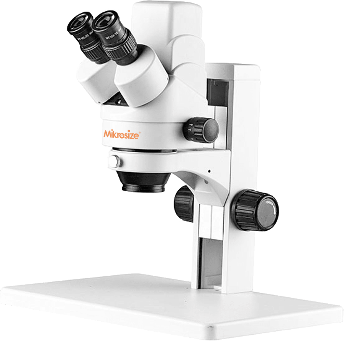
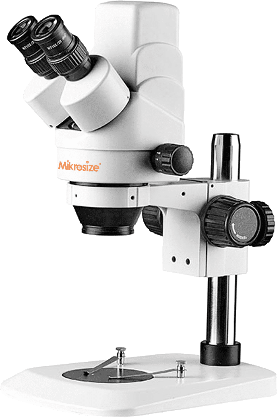
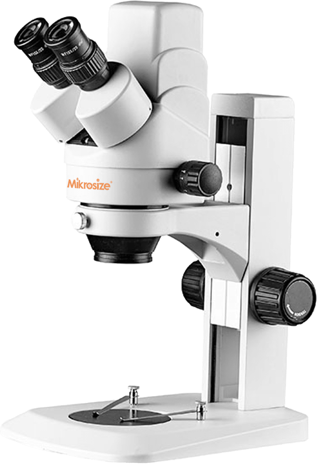
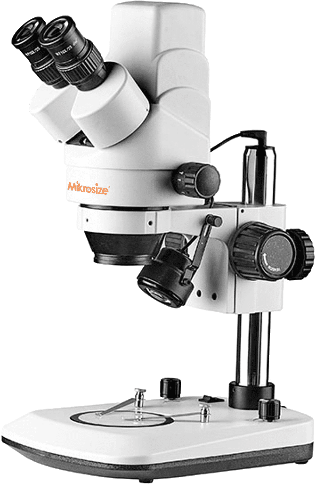
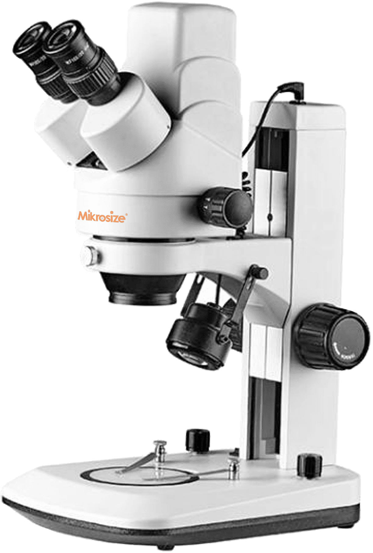
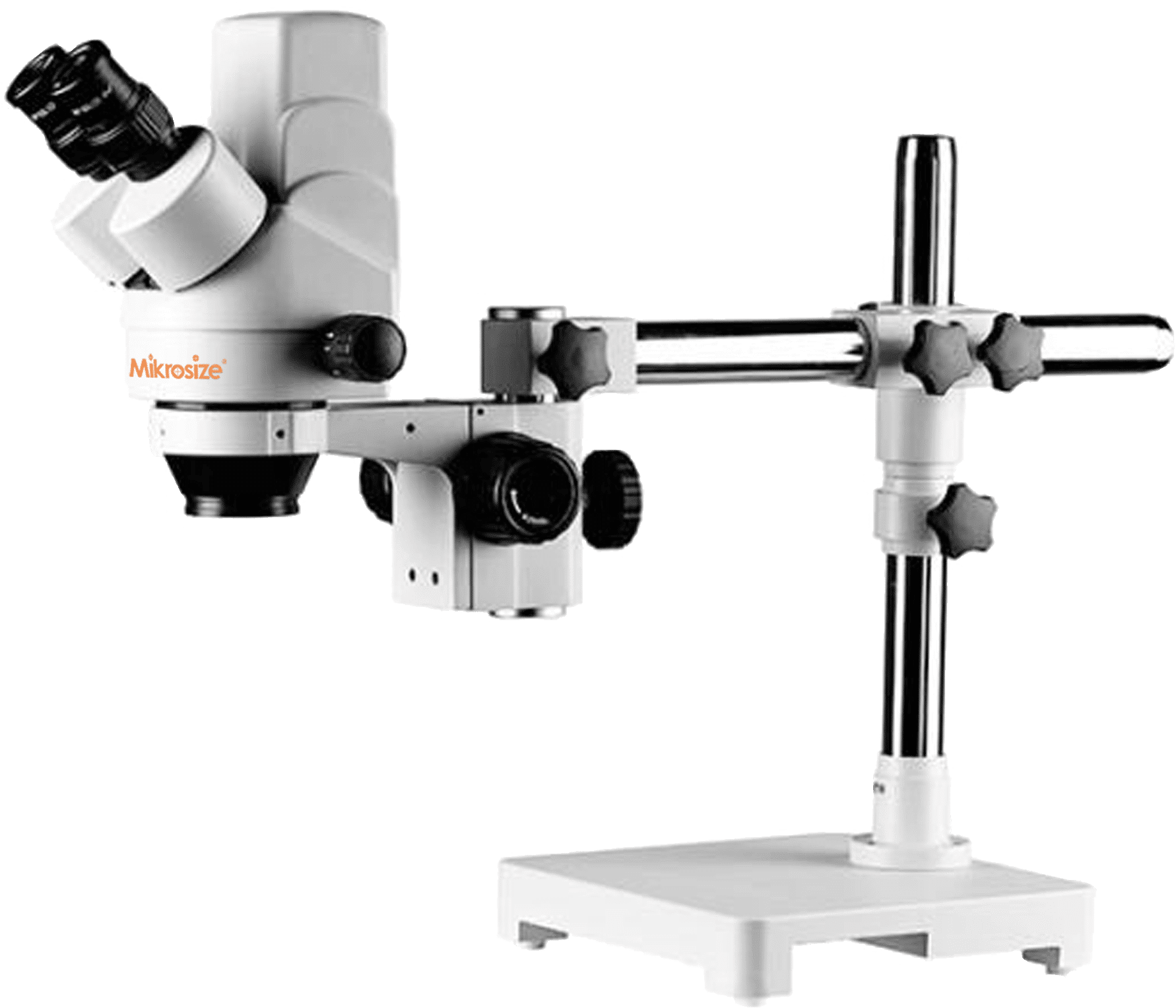
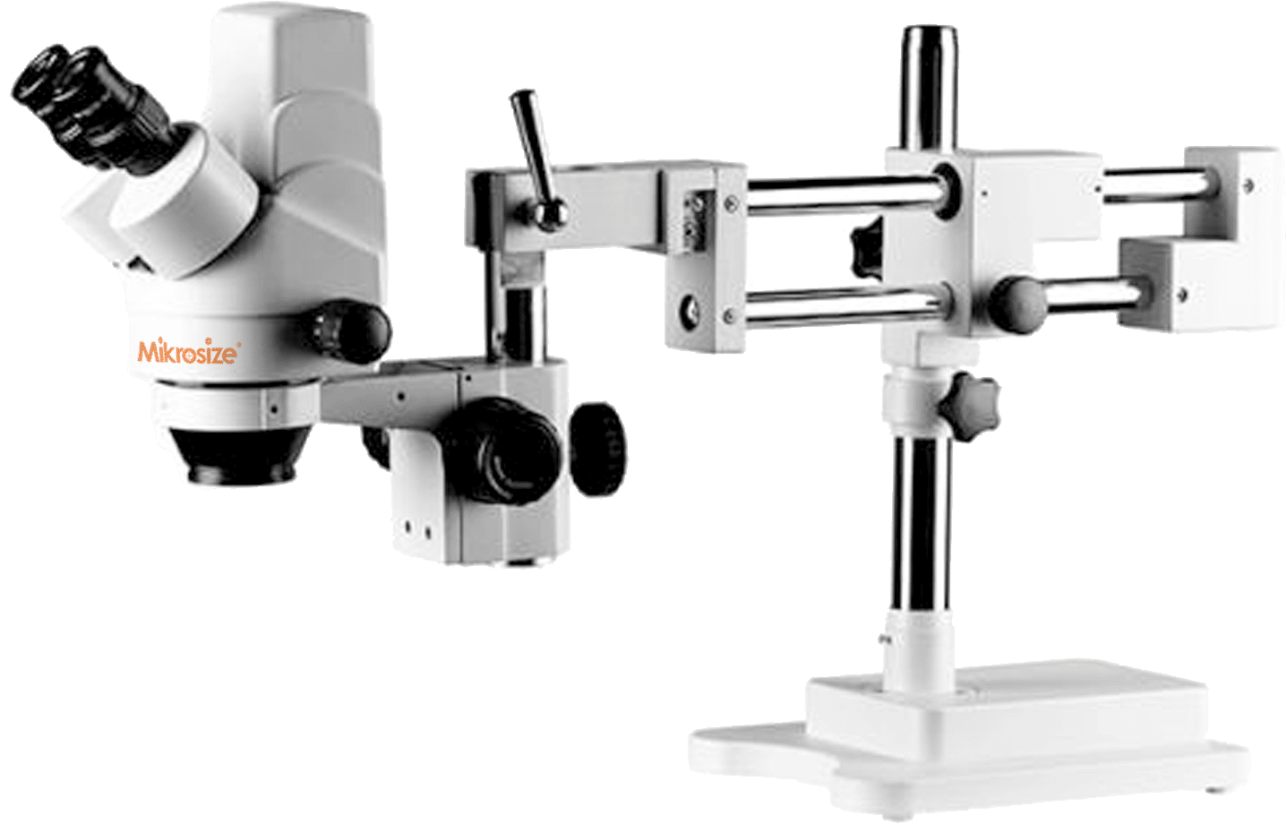
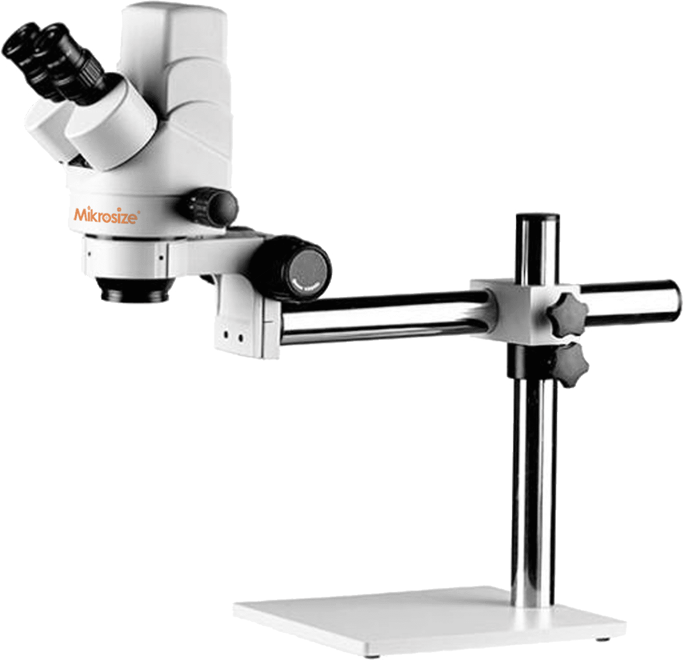
iMetal-40UP Metallographic Microscope
Scan QR
Scan QR
.png)
-1.jpg)
-1.jpg)
-1.jpg)
-1.jpg)
-1.jpg)
.jpg)
.jpg)
.jpg)
IMetal 40UP(1)
IMetal 40UP图(2) 1
IMetal 40UP图(3) 1
IMetal 40UP图(4) 1
IMetal 40UP图(5) 1
IMetal 40UP图(6) 1
IMetal 40UP图(7)
IMetal 40UP图(8)
IMetal 40UP图(9)
Video Demonstration
Product Features & Applications
Product Features
- Equipped with an infinite-distance chromatic aberra- tion correction system and a semi-reversed objective lens, combined with multiple observation modes and a high-resolution camera, the imaging is clear and sharp, with both details and contrast.
- The differential interference function can convert minute height differences into three-dimensional relief images, accurately detecting hidden defects such as LCD conductive particles and wafer scratches.
- The Mikrosize software supports automatic measure- ment, image stitching and report generation. The du- al-control design of the electric objective lens turnta- ble enhances the detection efficiency.
- The ergonomic frame is equipped with a wide-voltage system, a 4-inch loading platform and a long-work- ing-distance objective lens, which is suitable for vari- ous industrial samples and environments.
- The objective lens, camera pixels, observation tube, etc. can be selected as needed. It supports post-pro- cessing function upgrades to meet the customized re- quirements in various fields such as semiconductors and materials.
Product Applications
- Observation of dislocation pits and step flow defects on the external extension film, identi- fication of nanoscale undulations using DIC technology, which helps improve yield.
- Inspect the sharp edges and burrs of the cut, as well as surface scratches, analyze the voids in the packaging material, and ensure the performance and lifespan of the chip.
- Adapted for MLCC slice detection, it enables observation of the distribution of the elec- trode layer and the interface with the dielectric, and helps identify potential short-circuit hazards.
- Perform microscopic observation on the circuit board slices to evaluate the quality of the solder joints and the defects of the substrate materials.
- Observe the grains and grain boundaries of materials such as metals and ceramics, evalu- ate the heat treatment effect, and provide a basis for material optimization.
Technical Specifications
| Optical system | Infinite distance chromatic aberration correction optical system |
| Optical Magnification | 50X-500X(Optional 1000X) |
| Digital Magnification Factor | 150X-1500X(21.5-inch monitor) combined with a 100X objective lens, the magnification can reach 3000X |
| Industrial Camera | 5 million pixels, 1/1.8-inch color Sony industrial chip (optional 6.3 million and 20 million pixels) |
| Observation Tube | Inverted image, infinite distance hinge three-way eyepiece, interpupillary distance adjustment: 50mm - 76mm, two-stage light transmission ratio binoculars: 3 days = 100:0 |
| Eyepiece | High magnification and wide field eyepiece SWH10X-H/23mm, with adjustable viewing angle |
| Objective Lens | Infinite long working distance bright-dark field half-complex achromatic metallographic objective 5X NA 0.15 WD 14.8 |
| Infinity long working distance bright-dark field half-complex achromatic metallographic objective 10X NA 0.30 WD 8.5. | |
| Infinite long working distance bright-field and dark-field half-complex achromatic metallographic objective 20X NA 0.40 WD 11.9 | |
| Infinite long working distance bright-field and dark-field half-complex achromatic metallographic objective 50X NA 0.75 WD 3.0 | |
| Infinity long working distance bright-field and dark-field half-complex achromatic metallographic objective 100X NA 0.90 WD 1.0 (optional) | |
| Nosepiece | Manual five-hole objective turret / Electric bright-field and dark-field 5-hole converter (with DIC slot), with physical buttons and dual control via software. |
| Rack | Transmissive reflection frame, low-hand position coarse-fine coaxial focusing mechanism. Coarse adjustment travel 35mm, fine adjustment accuracy 0.001mm. Equipped with a regulating tension device to prevent sliding and a random upper limit position device. It is equipped with a 100-240V wide-voltage system and adopts digital dimming. It also has functions for setting and resetting the light intensity. |
| Workbench | 4-inch worktable, platform area 310*240mm, moving range: 100mm X 100mm mechanical platform, X and Y directions are coaxially adjustable. |
| Collimator | Swing-out type achromatic collimating mirror (N.A. 0.9). |
| Reflective Lighting Device | Ambient and shadow field reflective lighting device, with variable aperture diaphragm, field diaphragm, adjustable center position, with filter slot, with polarizer/linearizer slot. |
| Lamp Chamber | 5W adjustable LED lighting chamber, suitable for both transmission and reflection, with a preset center. |
| Video Interface | Photography and video accessory: 0.65X, C-type interface. |
| Polarization Component | Polarizer plate, 360° rotating polarizing plate. |
Standard Configuration
| Name | Qty | Photo | |
| Host Machine | 1pc | -15-300x240.jpg) |
|
| SWH10X-H/23mm Eyepiece | 2pcs | -15-300x207.jpg) |
|
| Lighting Fixture | 1pc | ||
| Objective lens | 5X NA0.15 WD14.8 | 1pc | -13-300x95.jpg) |
| 10X NA0.30 WD8.5 | 1pc | ||
| 20X NA0.40 WD11.9 | 1pc | ||
| 50X NA0.75 WD3.0 | 1pc | ||
| Nosepiece | 1pc | -9-300x179.jpg) |
|
| Lamp Chamber | 1pc | -8-199x300.jpg) |
|
| Workbench | 1pc | -7-300x247.jpg) |
|
| Glass Workbench | 1pc | -7-300x255.jpg) |
|
| 0.65x C-Type Camera Interface | 1pc | -6-259x300.jpg) |
|
| Polarization Component | 1pc | -6-300x148.jpg) |
|
| Trinocular Observation Head | 1pc | -4-300x124.jpg) |
|
| 500,000 Units Of 1/1.8-Inch Color Sony Industrial Camera With Chip Technology | 1pc | -4-300x296.jpg) |
|
| Instruction Manual | 1pc | -2-212x300.jpg) |
|
| Mikrosize Microscopic Analysis Software | 1pc | -2-300x209.jpg) |
|
| Hexagonal Wrench Set | 1pc | -2-300x135.jpg) |
|
| High-Precision Micrometer, With A Graduation Value Of 0.01mm | 1pc | -2-300x226.jpg) |
|
| Cleaning Set | 1pc | ||
| Dust Cover | 1pc | -2-300x217.jpg) |
|
| Power Cord | 1pc | -2-300x173.jpg) |
|
Contact Us
Get in touch for product information, quotes, or technical support
Call us
+86-0553-2836939
Email us
mikrosize@mikrosize.com